In der Halbleiterfertigung ist die Methode, mit der Siliziumblöcke in die in der Elektronik verwendeten Wafer zerlegt werden, ein entscheidender Faktor für die Effizienz der Produktion und die Qualität des Endprodukts. Die fortschrittlichen Drahtschneidetechniken haben diesen Prozess revolutioniert und gewährleisten, dass die Industrie mit der ständig steigenden Nachfrage nach kleineren, leistungsfähigeren elektronischen Geräten Schritt halten kann. Dieser Artikel befasst sich mit den innovativen Ansätzen des Drahtschneidens und geht insbesondere darauf ein, wie diese Methoden die Ausbeute und Qualität verbessert haben.
Im Kern geht es bei der Drahtschneidetechnik um Präzision und Effizienz. Traditionell wurden bei diesem Verfahren Siliziumblöcke mit einer Drahtsäge durchtrennt, eine Methode, die zwar effektiv war, aber in Bezug auf den Materialverlust und die Qualität des Schnitts viel Raum für Verbesserungen ließ. Die Einführung fortschrittlicher Drahtschneidetechniken war ein Wendepunkt, der die Herstellung dünnerer Wafer ermöglichte und den Materialverlust erheblich reduzierte.

Der Weg vom Drahtschneiden mit Slurry zum Einsatz von Diamantdrahtschneiden stellt einen bedeutenden Sprung nach vorn in der Branche dar. Jede Stufe dieser Entwicklung brachte Verbesserungen in Bezug auf Geschwindigkeit, Effizienz und Abfallvermeidung mit sich und gipfelte in einem Verfahren, das nicht nur die Anforderungen der heutigen Halbleiterindustrie erfüllt, sondern auch die Grundlage für künftige Innovationen bildet.
Vor allem das Schneiden mit Diamantdraht hat sich zu einer herausragenden Technik entwickelt, da es Siliziumblöcke mit unvergleichlicher Geschwindigkeit und Präzision durchtrennt. Bei dieser Methode wird ein mit Diamantpartikeln beschichteter Draht zum Schneiden verwendet, wodurch der Materialverlust minimiert und dünnere und hochwertigere Wafer als je zuvor hergestellt werden können.
Trotz ihrer Fortschritte ist die Drahtschneidetechnik nicht frei von Herausforderungen. Probleme wie Drahtverschleiß und die mit dem Schneiden mit Diamantdraht verbundenen Betriebskosten können die Gesamteffizienz des Prozesses beeinträchtigen. Darüber hinaus ist die Aufrechterhaltung der Integrität der Waferoberfläche während des Schneidens ein ständiges Anliegen, da jegliche Unvollkommenheit die Leistung des Endprodukts erheblich beeinträchtigen kann.
Mehrere Branchenführer haben Pionierarbeit beim Einsatz fortschrittlicher Drahtschneidetechnologien geleistet und dabei erhebliche Verbesserungen bei Ertrag und Qualität erzielt. Diese Erfolgsgeschichten sind ein Beweis für das Potenzial dieser Techniken, die Halbleiterfertigung zu verändern.
Die Zukunft der Drahtschneidetechnik sieht rosig aus, denn die laufenden Forschungs- und Entwicklungsanstrengungen konzentrieren sich darauf, den Prozess noch effizienter und nachhaltiger zu gestalten. Innovationen bei den Drahtmaterialien und Schneidetechniken versprechen, die Ausbeute und Qualität von Siliziumwafern weiter zu verbessern und sicherzustellen, dass die Halbleiterindustrie auch weiterhin die wachsende Nachfrage nach elektronischen Hochleistungsgeräten befriedigen kann.
Einführung in das Schneiden von Siliziumbarrendraht
Stellen Sie sich eine Welt vor, in der die Elektronik, die Ihr tägliches Leben versorgt, noch effizienter, kompakter und billiger ist. Diese Welt ist gar nicht so weit entfernt, wie Sie vielleicht denken, und sie wird durch Fortschritte in einem Verfahren eingeleitet, von dem Sie vielleicht noch nie gehört haben: das Schneiden von Siliziumbarren. Dieses Verfahren ist der unbesungene Held der Halbleiterindustrie, ein Bereich, der so fortschrittlich ist wie die Klingen, die bei dieser wichtigen Technik verwendet werden.
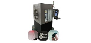
Das ist der Kern, Schneiden von Siliziumbarren-Draht ist ein Verfahren, mit dem Siliziumblöcke in dünne Wafer geschnitten werden, die die Grundlage für praktisch jedes elektronische Gerät bilden, das Sie benutzen - von Ihrem Smartphone bis zu Ihrem Laptop. Die Präzision und Effizienz dieses Prozesses wirken sich direkt auf die Qualität und die Kosten des Endprodukts aus und sind daher ein entscheidender Schritt in der Halbleiterherstellung.
Die Technologie hat sich von ihren rudimentären Anfängen zu hoch entwickelten Methoden entwickelt. Herkömmliche Sägeverfahren waren langsam und verschwenderisch, und es ging eine beträchtliche Menge an wertvollem Silizium im Sägemehl verloren. Einführung Diamantdrahtschneidenein Wendepunkt in der Branche. Bei diesem Verfahren wird ein dünner, mit Diamantpartikeln beschichteter Draht verwendet, der durch Siliziumblöcke schneidet wie ein heißes Messer durch Butter, wodurch der Materialabfall erheblich reduziert und die Effizienz des Schneidprozesses verbessert wird.
Aber warum ist das für Sie wichtig? Im Wesentlichen bedeuten die Fortschritte in der Drahtschneidetechnik, dass die Hersteller mehr Chips pro Siliziumbarren produzieren können, was zu billigerer Elektronik und schnelleren technologischen Fortschritten führen kann. Außerdem eröffnet die Möglichkeit, dünnere Wafer zu schneiden, ohne Abstriche bei der Festigkeit oder Qualität zu machen, die Tür zu neuen Innovationen bei Design und Funktionalität der Elektronik.
Aber es läuft nicht alles glatt. Der Prozess des Drahtschneidens von Siliziumblöcken ist mit einer Reihe von Herausforderungen verbunden, angefangen bei der Abnutzung der Schneiddrähte bis hin zur erforderlichen Präzision, um die Integrität der Waferoberfläche zu erhalten. Diese Herausforderungen stehen im Mittelpunkt der Forschung und Entwicklung in diesem Bereich und verschieben die Grenzen dessen, was in der Halbleiterfertigung möglich ist.
Zusammenfassend lässt sich sagen, dass das Drahtschneiden zwar wie ein kleiner Teil des Puzzles der Halbleiterherstellung erscheinen mag, seine Auswirkungen aber alles andere als das sind. Im Hinblick auf eine Zukunft mit immer leistungsfähigeren und effizienteren elektronischen Geräten werden die Innovationen beim Schneiden von Siliziumbarren weiterhin eine entscheidende Rolle spielen. Wenn Sie also das nächste Mal über Ihr Smartphone streichen oder Ihren Computer hochfahren, denken Sie an die Spitzentechnologie, die das alles möglich gemacht hat.
Die Entwicklung der Drahtschneidetechniken
Der Weg der Drahtschneidetechniken in der Halbleiterindustrie ist eine lebendige Geschichte von Innovation und Anpassung. Von den rudimentären Anfängen bis zu den heutigen Hightech-Lösungen war die Entwicklung des Drahtschneidens durch eine Reihe von Durchbrüchen gekennzeichnet, die die Effizienz und Qualität der Siliziumwaferproduktion erheblich verbessert haben. Lassen Sie uns einen Blick auf die wichtigsten Meilensteine werfen, die diesen Weg geprägt haben.
Ursprünglich stützte sich die Industrie auf Schneiden von Drähten mit SchlammBei dieser Methode wurde ein mit einer abrasiven Aufschlämmung beschichteter Draht zum Schneiden von Siliziumblöcken verwendet. Diese Methode war zu ihrer Zeit zwar effektiv, hatte aber auch Nachteile wie langsame Schnittgeschwindigkeiten, hohen Materialverlust und Unregelmäßigkeiten in der Waferdicke.
- Einführung des Diamantdrahtschneidens: Die Einführung des Diamantdrahtschneidens hat die Branche grundlegend verändert, denn die mit Diamantpartikeln eingebetteten Drähte bieten eine unübertroffene Präzision und Effizienz. Diese Methode beschleunigte nicht nur den Schneidprozess, sondern verringerte auch den Materialverlust drastisch und läutete damit eine neue Ära in der Siliziumwaferproduktion ein.
- Fortschritte in der Drahttechnologie: Im Laufe der Zeit wurden auch die Diamantdrähte selbst erheblich verbessert. Innovationen bei der Diamantbindung und der Drahtstärke erhöhten die Haltbarkeit und Lebensdauer der Drähte und optimierten den Schneidprozess weiter.
- Automatisierungs- und Steuerungssysteme: Die Integration fortschrittlicher Kontrollsysteme mit Drahtschneidemaschinen ermöglichte ein noch nie dagewesenes Maß an Präzision und Konsistenz. Die Echtzeitüberwachung und -anpassung während des Schneidprozesses minimierte Fehler und maximierte die Waferqualität.
Diese evolutionären Schritte in der Drahtschneidetechnik haben zu einem Verfahren geführt, das nicht nur schneller und kostengünstiger, sondern auch umweltfreundlicher ist, da es die Abfallmenge erheblich reduziert. Insbesondere der Übergang vom Slurry- zum Diamantdrahtschneiden markiert einen entscheidenden Moment in der Geschichte der Branche und setzt neue Maßstäbe für Effizienz und Nachhaltigkeit.
Wenn wir in die Zukunft blicken, versprechen die laufenden Forschungs- und Entwicklungsarbeiten noch ausgefeiltere Drahtschneidetechniken hervorzubringen. Innovationen wie das lasergestützte Schneiden und das Drahtrecycling stehen kurz davor, die Möglichkeiten der Silizium-Wafer-Produktion neu zu definieren. Die Weiterentwicklung der Drahtschneidetechniken ist zweifellos ein Eckpfeiler des Fortschritts in der Halbleiterindustrie und führt uns in eine Zukunft, in der die Möglichkeiten ebenso grenzenlos wie aufregend sind.

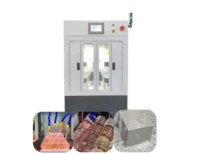
Verständnis für das Schneiden von Diamantdraht
Das Schneiden mit Diamantdraht ist ein Novum auf dem Gebiet des Schneidens von Siliziumblöcken und setzt einen neuen Standard für Präzision, Effizienz und minimalen Materialverlust. Im Gegensatz zu herkömmlichen Methoden, die auf Abrasivslurry beruhen, wird beim Diamantdrahtschneiden ein mit mikroskopisch kleinen Diamanten besetzter Draht zum Schneiden von Siliziumblöcken verwendet. Dieser innovative Ansatz beschleunigt nicht nur den Schneidprozess, sondern reduziert auch die Dicke des Abfallmaterials erheblich und maximiert so die Ausbeute aus jedem Ingot.
Doch was zeichnet das Schneiden von Diamantseilen aus? In erster Linie ist es die Geschwindigkeit. Da Diamant das härteste Material der Erde ist, kann er durch Silizium schneiden wie ein heißes Messer durch Butter, wodurch sich die Zeit, die zum Schneiden eines Barrens benötigt wird, drastisch verkürzt. Außerdem ist die Effizienz dieser Methode ist unvergleichlich. Die Möglichkeit, dünnere Wafer zu produzieren, bedeutet, dass mehr Chips aus einem einzigen Ingot hergestellt werden können, was ein großer Gewinn für Kosteneffizienz und Nachhaltigkeit ist.
Ein weiterer wesentlicher Vorteil ist die Qualität der hergestellten Wafer. Die Präzision des Diamantdrahtschneidens führt zu glatteren Oberflächen und einer gleichmäßigeren Dicke der Wafer. Dies ist entscheidend für die nachfolgenden Fertigungsschritte in der Halbleiterproduktion, bei denen jede Unregelmäßigkeit zu Mängeln im Endprodukt führen kann.
Der Übergang zur Diamantdrahtschneidetechnik war jedoch nicht ohne Herausforderungen. Die anfänglichen Einrichtungs- und Betriebskosten waren hoch, und die Beherrschung der Technik war mit einer Lernkurve verbunden. Darüber hinaus stellte die Haltbarkeit des Diamantseils selbst eine Herausforderung dar, da die Aufrechterhaltung der Schärfe und Integrität der mikroskopisch kleinen Diamanten für eine gleichbleibende Qualität und Effizienz unerlässlich war.
Trotz dieser Herausforderungen haben die Vorteile des Diamantdrahtschneidens dazu geführt, dass es die bevorzugte Wahl für das Schneiden von Siliziumblöcken ist. Die Technologie hat sich weiterentwickelt, wobei Verbesserungen bei der Haltbarkeit der Drähte und der Schneidausrüstung sie für die Hersteller zugänglicher und kostengünstiger gemacht haben. Heute steht das Schneiden mit Diamantdraht an der Spitze der Halbleiterherstellung und ermöglicht die Produktion dünnerer, hochwertigerer Wafer zu niedrigeren Kosten und mit geringeren Umweltauswirkungen.
Zusammenfassend lässt sich sagen, dass das Schneiden mit Diamantdraht einen bedeutenden Fortschritt in der Suche nach einer effizienteren, nachhaltigeren und kostengünstigeren Halbleiterfertigung darstellt. Seine Fähigkeit, qualitativ hochwertige Wafer schnell und mit minimalem Abfall herzustellen, hat es zu einer unverzichtbaren Technologie in der Branche gemacht. Mit Blick auf die Zukunft versprechen die kontinuierliche Weiterentwicklung und Verfeinerung des Diamantdrahtschneidens, die Grenzen des Möglichen in der Halbleiterproduktion weiter zu verschieben.
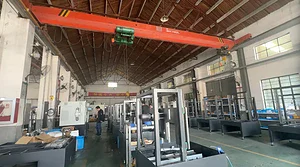
Herausforderungen beim Drahtschneiden von Siliziumblöcken
Die Umwandlung von Siliziumblöcken in die dünnen, polierten Wafer, die unsere elektronischen Geräte antreiben, ist mit vielen Herausforderungen verbunden. Die Drahtschneidetechnik hat sich zwar sprunghaft weiterentwickelt, ist aber nicht ohne Hürden. Diese Herausforderungen wirken sich nicht nur auf die Effizienz des Prozesses, sondern auch auf die Qualität des Endprodukts aus. Im Folgenden werden einige der wichtigsten Hindernisse beim Drahtschneiden von Siliziumblöcken näher erläutert.
1. Drahtverschleiß und -bruch: Eines der drängendsten Probleme beim Drahtschneiden ist der Verschleiß und Bruch des Drahtes selbst. Wenn der Draht den Siliziumblock durchschneidet, ist er einer enormen Belastung und Reibung ausgesetzt, was zu Verschleiß und schließlich zu einem Bruch führt. Dies verlangsamt nicht nur den Produktionsprozess, sondern erhöht auch die Betriebskosten, da der Draht häufig ausgetauscht werden muss.
2. Aufrechterhaltung der Integrität der Waferoberfläche: Die Sicherstellung der Glätte und Integrität der Waferoberfläche nach dem Schneiden ist eine weitere große Herausforderung. Unvollkommenheiten auf der Waferoberfläche können zu Defekten im endgültigen Halbleiterprodukt führen und dessen Leistung beeinträchtigen. Um ein Gleichgewicht zwischen Schneidgeschwindigkeit und Oberflächenqualität zu erreichen, ist eine präzise Steuerung der Drahtschneideparameter erforderlich.
3. Operative Kosten: Die Kosten für das Schneiden von Draht sind ein ständiges Problem für die Hersteller. Die mit dem Draht selbst verbundenen Kosten, insbesondere bei der Verwendung von diamantbeschichteten Drähten, der Energieverbrauch und die Wartung der Schneidausrüstung können sich summieren und die Gesamtrentabilität des Prozesses beeinträchtigen.
4. Materialverlust: Das Ziel eines jeden Schneidprozesses ist es, den Ertrag zu maximieren und gleichzeitig den Abfall zu minimieren. Beim Drahtschneiden spielen die Dicke des Drahtes und die Schnittfuge (die Breite des während des Schneidprozesses entfernten Materials) eine entscheidende Rolle bei der Bestimmung der Menge des verlorenen Materials. Dünnere Wafer bedeuten mehr Wafer pro Ingot, was jedoch auch zu Problemen bei der Handhabung und einem erhöhten Potenzial für Materialverluste führt.
- Dauerhaftigkeit des Drahtes: Suche nach Materialien und Beschichtungen, die die Lebensdauer der Drähte verlängern, ohne die Leistung zu beeinträchtigen.
- Oberflächenqualität: Entwicklung von Schneidetechniken, die die Oberflächenbeschädigung minimieren und weniger Nachbearbeitung erfordern.
- Kostenmanagement: Innovation von kosteneffizienteren Schneidelösungen ohne Abstriche bei Qualität und Effizienz.
- Abfallreduzierung: Verbesserung der Schnittpräzision zur Verringerung der Schnittfuge und des Materialverlusts und damit zur Verbesserung der Ausbeute.
Zusammenfassend lässt sich sagen, dass das Drahtschneiden von Siliziumblöcken zwar ein entscheidender Schritt bei der Herstellung von Halbleiterwafern ist, aber nicht ohne Probleme abläuft. Die Bewältigung dieser Probleme erfordert eine Kombination aus technologischer Innovation, Prozessoptimierung sowie kontinuierlicher Forschung und Entwicklung. Im Zuge der weiteren Entwicklung der Branche wird es entscheidend sein, Lösungen für diese Herausforderungen zu finden, um das Tempo des Fortschritts im Halbleitersektor beizubehalten.
Fallstudien: Erfolgsgeschichten im Drahtschneiden
Die Halbleiterindustrie ist ein Zeugnis für unermüdliche Innovation und technologischen Fortschritt. Unter den vielen Durchbrüchen sticht die Entwicklung des Drahtschneidens für Siliziumblöcke als bahnbrechend hervor. In diesem Abschnitt werden einige bemerkenswerte Fallstudien beleuchtet, die die Erfolgsgeschichte des Drahtschneidens unterstreichen und signifikante Sprünge bei Ertrag und Qualität aufzeigen.
Der Sprung von Unternehmen A zum Diamantdrahtschneiden: Unternehmen A, ein Pionier in der Halbleiterherstellung, wechselte vom traditionellen Drahtschneiden mit Schlamm zur Diamantdrahtschneidetechnik. Diese Umstellung führte zu einer satten Steigerung der Ausbeute um 30% aufgrund des geringeren Schnittspaltverlusts und der Möglichkeit, dünnere Wafer zu produzieren. Darüber hinaus konnten durch die Einführung des Diamantdrahtschneidens die Betriebskosten um 20% gesenkt werden, was eine perfekte Mischung aus Effizienz und Kosteneffizienz darstellt.
Die Innovation von Unternehmen B bei der Haltbarkeit von Drähten: Angesichts der Problematik des Drahtverschleißes, der häufig zu häufigen Auswechslungen und Ausfallzeiten führt, führte Unternehmen B eine revolutionäre Drahtbeschichtungstechnik ein. Diese Innovation verlängerte die Lebensdauer des Drahtes um 40%, erhöhte die betriebliche Effizienz und senkte die Gesamtbetriebskosten.
- Verbesserte Oberflächenintegrität: Verbesserte Drahtschneidetechniken haben auch zu einer besseren Oberflächenqualität der Wafer geführt, was den Bedarf an zusätzlicher Bearbeitung verringert und somit Zeit und Ressourcen spart.
- Materialerhaltung: Mit dem Aufkommen präziserer Schneideverfahren haben die Unternehmen über eine spürbare Verringerung des Siliziumabfalls berichtet, was zu einer nachhaltigeren Fertigungspraxis beiträgt.
Diese Erfolgsgeschichten sind keine Einzelfälle, sondern vielmehr Ausdruck eines allgemeinen Trends zu Innovation und Verbesserung in der Halbleiterindustrie. Die Einführung fortschrittlicher Drahtschneidetechnologien hat nicht nur die betriebliche Effizienz verbessert, sondern auch den Weg für die Entwicklung qualitativ hochwertiger Halbleitergeräte geebnet. Während sich die Branche weiter entwickelt, werden diese Fallstudien als Benchmarks für zukünftige technologische Fortschritte dienen.

Zukünftige Trends in der Drahtschneidetechnik
Die Landschaft der Drahtschneidetechnik steht kurz vor einer Revolution. Neue Trends und Innovationen versprechen, Effizienz, Nachhaltigkeit und Präzision bei der Verarbeitung von Siliziumblöcken neu zu definieren. Wenn wir in die Zukunft blicken, stehen mehrere wichtige Entwicklungen an, die die Branche verändern werden:
- Automatisierung und Robotik: Die Integration von Automatisierung und Robotik in den Drahtschneidebetrieb wird die Präzision und Konsistenz verbessern. Automatisierte Systeme können die Schneidparameter in Echtzeit anpassen, um optimale Effizienz und minimalen Ausschuss zu erzielen, was zu höheren Ausbeuten und niedrigeren Betriebskosten führt.
- Greener Cutting Solutions: Die ökologische Nachhaltigkeit gewinnt in der Halbleiterfertigung zunehmend an Bedeutung. Künftige Drahtschneidetechnologien können umweltfreundlichere Schneidmaterialien und -verfahren einsetzen, die den Einsatz schädlicher Chemikalien reduzieren und die Abfallmenge minimieren.
- Fortschrittliche Diamantdraht-Technologie: Es werden kontinuierliche Verbesserungen in der Diamantdrahttechnologie erwartet, einschließlich Innovationen in der Drahtzusammensetzung und im Design. Diese Fortschritte könnten den Materialverlust weiter verringern, die Schnittgeschwindigkeit erhöhen und die Lebensdauer des Drahtes verlängern, wodurch die Gesamtproduktivität gesteigert und die Kosten gesenkt werden könnten.
- Maschinelles Lernen und KI: Die Anwendung von maschinellem Lernen und künstlicher Intelligenz (KI) in Drahtschneideprozessen könnte zu erheblichen Verbesserungen bei der vorausschauenden Wartung, Prozessoptimierung und Qualitätskontrolle führen. Durch die Analyse von Daten aus dem Schneidprozess können KI-Algorithmen Anlagenausfälle vorhersagen, bevor sie auftreten, und die Schneidparameter für jeden einzelnen Barren optimieren, was eine gleichbleibende Qualität und eine Maximierung der Ausbeute gewährleistet.
- Hybride Schneidetechnologien: Die Entwicklung hybrider Schneidverfahren, die die Stärken verschiedener Schneidtechniken kombinieren, könnte neue Lösungen für Herausforderungen wie Drahtverschleiß und Oberflächenintegrität bieten. So könnte die Integration des Laserschneidens mit dem Sägen mit Diamantdraht eine präzise Steuerung des Schneidprozesses ermöglichen und die mechanische Belastung der Siliziumwafer verringern.
Mit der Entwicklung dieser Zukunftstrends wird die Drahtschneideindustrie einen Innovationsschub erleben, der zu effizienteren, nachhaltigeren und kostengünstigeren Herstellungsverfahren führen wird. Die kontinuierliche Weiterentwicklung der Drahtschneidetechnik wird nicht nur die Ausbeute und Qualität von Siliziumwafern verbessern, sondern auch das Wachstum der Halbleiterindustrie insgesamt fördern.
Häufig gestellte Fragen
- Was ist die Drahtschneidetechnik im Zusammenhang mit Siliziumblöcken?Die Drahtschneidetechnik, insbesondere im Bereich der Siliziumblöcke, ist ein präzisionsgesteuertes Verfahren, das in der Halbleiterindustrie eingesetzt wird. Dabei werden Siliziumrohlinge in dünne Wafer geschnitten, die als Grundlage für Halbleiterbauelemente dienen. Die Entwicklung vom traditionellen Schneiden mit Schlämmen zum innovativen Schneiden mit Diamantdraht hat die Effizienz erheblich gesteigert, den Materialabfall verringert und die Qualität der fertigen Wafer verbessert.
- Wie hat sich das Drahtschneiden im Laufe der Jahre entwickelt?Die Entwicklung der Drahtschneidetechnologie ist von ständiger Innovation geprägt, die von auf Schlamm basierenden Techniken zur Einführung des Diamantdrahtschneidens führte. Diese Entwicklung spiegelt das Streben nach höherer Produktivität, Kosteneffizienz und der Fähigkeit wider, dünnere, hochwertige Wafer mit minimalem Schnittfugenverlust herzustellen. Vor allem das Schneiden mit Diamantdraht hat das Verfahren durch seine unübertroffene Geschwindigkeit und Effizienz revolutioniert.
- Warum wird das Schneiden mit Diamantdraht den traditionellen Methoden vorgezogen?Das Schneiden mit Diamantdraht zeichnet sich durch seine außergewöhnliche Geschwindigkeit, Effizienz und die Fähigkeit aus, dünnere Wafer zu produzieren und gleichzeitig den Materialverlust zu minimieren. Bei dieser Methode wird ein mit Diamantpartikeln besetzter Draht zum Schneiden von Siliziumblöcken verwendet, wodurch die Abfallmenge verringert und die Ausbeute und Qualität der Wafer erheblich verbessert wird. Die Einführung dieses Verfahrens bedeutet einen großen Schritt in Richtung einer nachhaltigeren und kostengünstigeren Halbleiterherstellung.
- Welche Herausforderungen sind mit dem Drahtschneiden von Siliziumblöcken verbunden?Trotz seiner Fortschritte ist das Drahtschneiden von Silizium-Ingots nicht ohne Herausforderungen. Probleme wie die Abnutzung der Drähte, die Betriebskosten und die Aufrechterhaltung der Integrität der Wafer-Oberfläche stellen erhebliche Hürden dar. Diese Herausforderungen erfordern kontinuierliche Forschung und Innovation, um den Prozess zu verfeinern, die Haltbarkeit zu verbessern und die Produktion hochwertiger Halbleiterwafer zu gewährleisten.
- Können Sie uns einige Erfolgsgeschichten beim fortgeschrittenen Drahtschneiden nennen?In der Tat haben mehrere Branchenführer Pionierarbeit bei der Integration fortschrittlicher Drahtschneidetechnologien geleistet und bemerkenswerte Verbesserungen bei Effizienz, Ausbeute und Waferqualität erzielt. Diese Erfolgsgeschichten unterstreichen die transformative Wirkung des Diamantdrahtschneidens und anderer Innovationen, die neue Maßstäbe für die Halbleiterindustrie setzen und den Weg für zukünftige Fortschritte ebnen.
- Was sind die zukünftigen Trends in der Drahtschneidetechnik?Die Zukunft der Drahtschneidetechnik sieht vielversprechend aus. Neue Technologien und laufende Forschungsarbeiten zielen darauf ab, den Prozess noch effizienter und nachhaltiger zu gestalten. Innovationen wie das lasergestützte Schneiden und Entwicklungen in der Diamantdrahttechnologie werden voraussichtlich die Präzision, Geschwindigkeit und Umweltfreundlichkeit der Silizium-Wafer-Produktion weiter verbessern und eine spannende Ära für die Halbleiterindustrie einläuten.