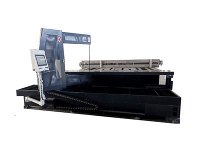
In the realm of semiconductor manufacturing, the method by which silicon ingots are sliced into the wafers used in electronics is a critical determinant of both the efficiency of production and the quality of the final product. Enter the advanced wire cutting techniques that have revolutionized this process, ensuring that the industry can keep pace with the ever-increasing demand for smaller, more powerful electronic devices. This article delves into the innovative approaches to wire cutting, specifically focusing on how these methods have enhanced yield and quality.
At its core, wire cutting technology is about precision and efficiency. Traditionally, this process involved using a wire saw to slice through silicon ingots, a method that, while effective, left much room for improvement in terms of material waste and the quality of the cut. The introduction of advanced wire cutting techniques has been a game-changer, allowing for the production of thinner wafers and reducing material loss significantly.

The journey from slurry-based wire cutting to the adoption of diamond wire cutting represents a significant leap forward in the industry. Each stage in this evolution brought with it improvements in speed, efficiency, and the reduction of waste, culminating in a process that not only meets the needs of today’s semiconductor industry but sets the stage for future innovations.
Diamond wire cutting, in particular, has emerged as a standout technique for its ability to slice through silicon ingots with unparalleled speed and precision. This method uses a wire coated in diamond particles to cut, minimizing material loss and producing wafers that are thinner and of higher quality than ever before possible.
Despite its advancements, wire cutting technology is not without its challenges. Issues such as wire wear and the operational costs associated with diamond wire cutting can impact the overall efficiency of the process. Additionally, maintaining the integrity of the wafer surface during cutting is a constant concern, as any imperfections can significantly affect the performance of the final product.
Several industry leaders have pioneered the use of advanced wire cutting technologies, demonstrating significant improvements in both yield and quality. These success stories serve as a testament to the potential of these techniques to transform the semiconductor manufacturing landscape.
The future of wire cutting technology looks bright, with ongoing research and development efforts focused on making the process even more efficient and sustainable. Innovations in wire materials and cutting techniques promise to further enhance the yield and quality of silicon wafers, ensuring that the semiconductor industry can continue to meet the growing demand for high-performance electronic devices.
Introduction to Silicon Ingot Wire Cutting
Imagine a world where the electronics that power your daily life are even more efficient, more compact, and cheaper. That world isn’t as far off as you might think, and it’s being ushered in by advances in a process you might never have heard of: silicon ingot wire cutting. This process is the unsung hero of the semiconductor industry, a field that’s as cutting-edge as the blades used in this vital technique.
At its core, silicon ingot wire cutting is a method used to slice silicon ingots into thin wafers, which are the foundation of virtually every electronic device you use—from your smartphone to your laptop. The precision and efficiency of this process directly impact the quality and cost of the final product, making it a critical step in semiconductor manufacturing.
The technology has evolved from its rudimentary beginnings to incorporate highly sophisticated methods. Traditional sawing methods were slow and wasteful, losing a substantial amount of precious silicon in the sawdust. Enter diamond wire cutting, a game-changer in the industry. This method uses a thin wire coated with diamond particles to slice through silicon ingots like a hot knife through butter, significantly reducing material waste and improving the efficiency of the cutting process.
But why does this matter to you? In essence, the advancements in wire cutting technology mean that manufacturers can produce more chips per silicon ingot, which can lead to cheaper electronics and more rapid advancements in technology. Plus, the ability to cut thinner wafers without sacrificing strength or quality opens the door to new innovations in electronics design and functionality.
However, it’s not all smooth sailing. The process of wire cutting silicon ingots faces its own set of challenges, from the wear and tear on the cutting wires to the need for precision in order to maintain the integrity of the wafer’s surface. These challenges are the frontlines of research and development in the field, pushing the boundaries of what’s possible in semiconductor manufacturing.
In conclusion, while wire cutting might seem like a small piece of the semiconductor manufacturing puzzle, its impact is anything but. As we look toward a future filled with ever more powerful and efficient electronic devices, the innovations in silicon ingot wire cutting will continue to play a pivotal role. So, the next time you swipe your smartphone or boot up your computer, spare a thought for the cutting-edge technology that made it all possible.
The Evolution of Wire Cutting Techniques
The journey of wire cutting techniques in the semiconductor industry is a vivid tale of innovation and adaptation. From its rudimentary beginnings to the high-tech solutions of today, the evolution of wire cutting has been marked by a series of breakthroughs that have significantly improved the efficiency and quality of silicon wafer production. Let’s dive into the key milestones that have shaped this journey.
Initially, the industry relied on slurry-based wire cutting, where a wire coated with an abrasive slurry was used to slice through silicon ingots. This method, though effective for its time, was fraught with drawbacks such as slow cutting speeds, high material wastage, and inconsistencies in wafer thickness.
- Introduction of Diamond Wire Cutting: A game-changer in the field, diamond wire cutting introduced wires embedded with diamond particles, offering unmatched precision and efficiency. This method not only accelerated the cutting process but also drastically reduced material loss, heralding a new era in silicon wafer production.
- Advancements in Wire Technology: Over time, the diamond wires themselves underwent significant improvements. Innovations in diamond bonding and wire strength enhanced the durability and lifespan of the wires, further optimizing the cutting process.
- Automation and Control Systems: The integration of advanced control systems with wire cutting machinery allowed for unprecedented levels of precision and consistency. Real-time monitoring and adjustments during the cutting process minimized errors and maximized wafer quality.
These evolutionary steps in wire cutting technology have culminated in a process that is not only faster and more cost-effective but also environmentally friendly, as it significantly reduces waste. The transition from slurry-based to diamond wire cutting, in particular, marks a pivotal moment in the industry’s history, setting new standards for efficiency and sustainability.
As we look to the future, the ongoing research and development promise to usher in even more sophisticated wire cutting techniques. Innovations such as laser-assisted cutting and wire recycling are on the horizon, poised to redefine what’s possible in silicon wafer production. The evolution of wire cutting techniques is, without doubt, a cornerstone of the semiconductor industry’s progress, driving us towards a future where the possibilities are as limitless as they are exciting.
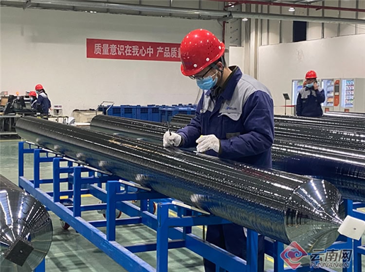
Understanding Diamond Wire Cutting
Diamond wire cutting is a game-changer in the field of silicon ingot slicing, setting a new standard for precision, efficiency, and minimal material wastage. Unlike traditional methods that relied on abrasive slurry, diamond wire cutting uses a wire embedded with microscopic diamonds to slice through silicon ingots. This innovative approach not only accelerates the cutting process but also significantly reduces the thickness of the waste material, thereby maximizing the yield from each ingot.
But what makes diamond wire cutting stand out? First and foremost, it’s the speed. Diamond, being the hardest material on Earth, can cut through silicon like a hot knife through butter, drastically reducing the time it takes to slice an ingot. Moreover, the efficiency of this method is unparalleled. The ability to produce thinner wafers means more chips can be manufactured from a single ingot, which is a big win for cost-effectiveness and sustainability.
Another significant advantage is the quality of the wafers produced. The precision of diamond wire cutting results in smoother surfaces and more uniform thickness across the wafers. This is crucial for the subsequent manufacturing steps in semiconductor production, where any imperfection can lead to defects in the final product.
However, the transition to diamond wire cutting technology was not without its challenges. The initial setup and operational costs were high, and there was a learning curve involved in mastering the technique. Moreover, the durability of the diamond wire itself posed a challenge, as maintaining the sharpness and integrity of the microscopic diamonds was essential for consistent quality and efficiency.
Despite these challenges, the benefits of diamond wire cutting have made it the preferred choice for silicon ingot slicing. The technology has evolved, with improvements in wire durability and cutting equipment making it more accessible and cost-effective for manufacturers. Today, diamond wire cutting is at the forefront of semiconductor manufacturing, enabling the production of thinner, higher-quality wafers at a lower cost and with less environmental impact.
In summary, diamond wire cutting represents a significant leap forward in the quest for more efficient, sustainable, and cost-effective semiconductor manufacturing. Its ability to produce high-quality wafers quickly and with minimal waste has made it an indispensable technology in the industry. As we look toward the future, the continued evolution and refinement of diamond wire cutting promise to keep pushing the boundaries of what’s possible in semiconductor production.
Challenges in Wire Cutting of Silicon Ingots
The journey of transforming silicon ingots into the thin, polished wafers that power our electronic devices is fraught with challenges. While wire cutting technology has advanced leaps and bounds, it’s not without its hurdles. These challenges not only affect the efficiency of the process but also the quality of the final product. Let’s delve into some of the significant obstacles faced during the wire cutting of silicon ingots.
1. Wire Wear and Breakage: One of the most pressing issues in wire cutting is the wear and breakage of the wire itself. As the wire slices through the silicon ingot, it undergoes tremendous stress and friction, leading to wear and, eventually, breakage. This not only slows down the production process but also increases operational costs due to the need for frequent wire replacements.
2. Maintaining Wafer Surface Integrity: Ensuring the smoothness and integrity of the wafer surface post-cutting is another significant challenge. Imperfections on the wafer surface can lead to defects in the final semiconductor product, impacting its performance. Achieving a balance between cutting speed and surface quality requires precise control over the wire cutting parameters.
3. Operational Costs: The cost of wire cutting operations is a constant concern for manufacturers. The expenses associated with the wire itself, especially when using diamond-coated wires, energy consumption, and maintenance of the cutting equipment, can add up, affecting the overall profitability of the process.
4. Material Loss: The goal of any cutting process is to maximize yield while minimizing waste. In wire cutting, the thickness of the wire and the kerf (the width of material removed during the cutting process) play crucial roles in determining the amount of material lost. Thinner wafers mean more wafers per ingot, but this also leads to challenges in handling and increased potential for material loss.
- Wire Durability: Finding materials and coatings that extend the life of the wire without compromising performance.
- Surface Quality: Developing cutting techniques that minimize surface damage and require less post-cutting processing.
- Cost Management: Innovating more cost-effective cutting solutions that do not sacrifice quality or efficiency.
- Waste Reduction: Enhancing cutting precision to reduce kerf and material loss, thereby improving yield.
In conclusion, while wire cutting of silicon ingots is a critical step in the production of semiconductor wafers, it is not without its challenges. Addressing these issues requires a combination of technological innovation, process optimization, and ongoing research and development. As the industry continues to evolve, finding solutions to these challenges will be key to maintaining the pace of progress in the semiconductor sector.
Case Studies: Success Stories in Wire Cutting
The semiconductor industry is a testament to relentless innovation and technological advancement. Among the many breakthroughs, the evolution of wire cutting for silicon ingots stands out as a game-changer. This section shines a light on a few remarkable case studies that underscore the success stories in wire cutting, demonstrating significant leaps in yield and quality.
Company A’s Leap to Diamond Wire Cutting: Company A, a pioneer in semiconductor manufacturing, transitioned from traditional slurry-based wire cutting to diamond wire cutting technology. This shift resulted in a whopping 30% increase in yield due to the reduced kerf loss and the ability to produce thinner wafers. Moreover, the implementation of diamond wire cutting slashed operational costs by 20%, showcasing a perfect blend of efficiency and cost-effectiveness.
Company B’s Innovation in Wire Durability: Facing the challenge of wire wear, which often leads to frequent replacements and downtime, Company B introduced a revolutionary wire coating technique. This innovation significantly extended the wire’s lifespan by 40%, enhancing operational efficiency and reducing the total cost of ownership.
- Enhanced Surface Integrity: Improved wire cutting techniques have also led to better surface quality of the wafers, reducing the need for additional processing and thus saving time and resources.
- Material Conservation: With the advent of more precise cutting methods, companies have reported a noticeable reduction in silicon waste, contributing to more sustainable manufacturing practices.
These success stories are not just isolated incidents but rather indicative of a broader trend towards innovation and improvement in the semiconductor industry. The adoption of advanced wire cutting technologies has not only enhanced operational efficiency but also paved the way for the development of superior-quality semiconductor devices. As the industry continues to evolve, these case studies will serve as benchmarks for future technological advancements.
Future Trends in Wire Cutting Technology
The landscape of wire cutting technology is on the brink of a revolution, with emerging trends and innovations promising to redefine efficiency, sustainability, and precision in the processing of silicon ingots. As we look to the future, several key developments stand poised to transform the industry:
- Automation and Robotics: The integration of automation and robotics into wire cutting operations is set to enhance precision and consistency. Automated systems can adjust cutting parameters in real-time for optimal efficiency and minimal waste, leading to higher yield rates and lower operational costs.
- Greener Cutting Solutions: Environmental sustainability is becoming increasingly important in semiconductor manufacturing. Future wire cutting technologies may employ more eco-friendly cutting materials and processes, reducing the use of harmful chemicals and minimizing waste.
- Advanced Diamond Wire Technology: Continuous improvements in diamond wire technology are expected, including innovations in wire composition and design. These advancements could further reduce material loss, increase cutting speed, and extend wire life, thereby enhancing overall productivity and reducing costs.
- Machine Learning and AI: The application of machine learning and artificial intelligence (AI) in wire cutting processes could lead to significant improvements in predictive maintenance, process optimization, and quality control. By analyzing data from the cutting process, AI algorithms can predict equipment failures before they occur and optimize cutting parameters for each ingot, ensuring consistent quality and maximizing yield.
- Hybrid Cutting Technologies: The development of hybrid cutting methods, combining the strengths of different cutting techniques, could offer new solutions for challenges such as wire wear and surface integrity. For example, integrating laser cutting with diamond wire sawing could enable precise control over the cutting process, reducing mechanical stress on the silicon wafers.
As these future trends develop, the wire cutting industry is set to witness a surge in innovation, leading to more efficient, sustainable, and cost-effective manufacturing processes. The continuous evolution of wire cutting technology will not only enhance the yield and quality of silicon wafers but also drive the growth of the semiconductor industry as a whole.
Часто задаваемые вопросы
- What is wire cutting technology in the context of silicon ingots?Wire cutting technology, especially in the realm of silicon ingots, is a precision-driven process used in the semiconductor industry. It involves slicing silicon ingots into thin wafers, serving as the foundation for semiconductor devices. The evolution from traditional slurry-based cutting to innovative diamond wire cutting has significantly enhanced efficiency, reduced material waste, and improved the quality of the final wafers.
- How has wire cutting evolved over the years?The journey of wire cutting technology has been marked by continuous innovation, moving from slurry-based techniques to the adoption of diamond wire cutting. This evolution reflects a quest for higher productivity, cost-effectiveness, and the ability to produce thinner, high-quality wafers with minimal kerf loss. Diamond wire cutting, in particular, has revolutionized the process by offering unmatched speed and efficiency.
- Why is diamond wire cutting preferred over traditional methods?Diamond wire cutting stands out for its exceptional speed, efficiency, and the ability to produce thinner wafers while minimizing material loss. This method uses a wire embedded with diamond particles to slice through silicon ingots, reducing the amount of waste produced and significantly improving the yield and quality of the wafers. Its adoption signifies a leap towards more sustainable and cost-effective semiconductor manufacturing.
- What challenges are associated with wire cutting of silicon ingots?Despite its advancements, wire cutting of silicon ingots is not without its challenges. Issues such as wire wear and tear, operational costs, and maintaining the integrity of the wafer surface pose significant hurdles. These challenges necessitate ongoing research and innovation to refine the process, enhance durability, and ensure the production of high-quality semiconductor wafers.
- Can you share some success stories in advanced wire cutting?Indeed, several industry leaders have pioneered the integration of advanced wire cutting technologies, showcasing remarkable improvements in efficiency, yield, and wafer quality. These success stories highlight the transformative impact of diamond wire cutting and other innovations, setting new benchmarks for the semiconductor industry and paving the way for future advancements.
- What are the future trends in wire cutting technology?The future of wire cutting technology looks promising, with emerging technologies and ongoing research aimed at making the process even more efficient and sustainable. Innovations such as laser-assisted cutting and developments in diamond wire technology are expected to further enhance the precision, speed, and eco-friendliness of silicon wafer production, heralding an exciting era for the semiconductor industry.

